 LC5910S Calculation Tool
Before Using This Tool
- This tool is designed to help you calculate Peripheral Circuit Constants, Design Values and Power Losses in a LC5910S LED Driver system.
- Before using this tool, please read the LC5910S data sheet.
- All the device characteristic parameters are typical values at TJ = 25 ℃.
- All the values automatically entered into the text boxes in the Calculation Conditions pane are default values (for reference).
- All the values calculated by this tool are reference values, NOT guaranteed values.
- This tool has NOT been guaranteed to work properly on all browsers.
Runing a Calculation
- In the Calculation Conditions pane, move the slider to set a numerical value in each field.
- To run a calculation, click the Calculate button.
− Move the slider to enter or adjust a numerical value in each text box.
− To enter a numecial value directly, click or tap (hereafter “click”) in the field.
− When using a keyboard, click to select the slider thumb, and then use arrow keys (left and right) on your keyboard to move the slider.
− To run a new calculation after you made any changes to the values entered, click the Calculate button again.
− If the tool displays an error calculation result after you click the Calculate button, see “Troubleshooting” below.
Reset Button
- Resets all the values entered in the Calculation Conditions pane.
- Resets all the positions of the slider thumbs in the Calculation Conditions pane to their default settings.
- Makes no change to the values in the Calculation Results pane.
Troubleshooting
- SYMPTOM: " NaN " is displayed in the Calculation Results pane.
− Either one or more fields in the Calculation Conditions pane are left blank.
− Any of the user-entered values contains numerals or characters other than half-width digits or a half-width period ( . ).
− Any of the user-entered values contains a half-width period ( . ) at an invalid position.
Examples: “ .3.4 ”, “ .2. ”, “ 0.6. ”
Examples: “ .3.4 ”, “ .2. ”, “ 0.6. ”
The Basics Explained
Basic Circuit Connection
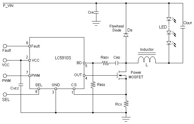
Description of circuit symbols in Basic Circuit Connection
- CVCC : Input Smoothing Capacitor
- COUT : Output Smoothing Capacitor for VLED
- CBD : Coupling capacitor for Bottom Detection (Default value ≅ 15 pF to 100 pF, Please adjust it in the real operation while watching the waveform. )
- RBD1 : Voltage Dividing Resistor for Bottom Detection and Bottom Adjustment " upper " ( Default value ≅ 63 kΩ, Please adjust it in the real operation while watching the waveform. )
- RBD2 : Voltage Dividing Resistor for Bottom Detection and Bottom Adjustment " lower " ( Default value ≅ 2.2 kΩ, Please adjust it in the real operation while watching the waveform. )
- RCS : LED Current Setting Resistor
- DS : Freewheel diode ( Regenerative diode )
- PowerMOSFET : External PowerMOSFET
- Inductor L : Inductance L Value
Inductance L Value Calculation Procedure
- Enter the wished target frequency value into the text box of Target Frequency FSW.
- Click the Calculate button and calculate target inductance L value.
- Refer to the Inductor Manufacturer's Catalog.
- The Switching Frequency Fsw decreases due to the Delay Time associated with bottom detection. For this reason, please select a value slightly smaller than the calculation result.
- Enter the user-selected inductance L value into the text box of Inductance L Value Setting.
- Click the Calculate Button and recalculate Switching Frequency according to the user-selected inductance L value.
- Please confirm that it is close to the wished frequency.
Supplementary matter
- VIN is the main power supply of the LED driver circuit.
- VLED is the voltage across the LED-String.
- ILED is the average current of the LED-String.
- As for the target frequency, please enter the wished frequency, but if it is too high, the Switching losses will increase.
- The entering values of the power supply voltage VCC for LC5910S and the Qg of the external PowerMOSFET are used for loss calculation in the LC5910S.
- The Cds entering value of the external PowerMOSFET is used to calculate the Turn-ON Delay Time.
- The RDS(ON) and the Turn-OFF Ttransition Time Tf are used to calculate the Switching loss in the external PowerMOSFET.
- The VF entering value of the Freewheel Diode Ds is used to calculate the conduction loss in the Freewheel Diode Ds.
- Regarding the setting of the target output ripple voltage VLED(Ripple), please enter the value how do you want to suppress the output ripple voltage magnitude ? ( Unit : mV peak to peak )
- The entering values of CIN Reflux Current Peak Value, CIN Reflux Current Conduction Period T1, CIN Discharge Current Conduction Period T2 are used for approximating the Ripple Current of CIN.
- The corrected-Switching-Cycle T in the Calculation Results pane is the sum of the corrected-ON-period Ton and the corrected-OFF-period Toff that is added the Delay Time.
- In the calculation results pane, the ESR requirement value and ripple current of the output smoothing capacitor CO are calculated by the user selected inductance L value.
- To calculate the ripple current that flows in CIN, confirm the inductor current IL in the real-operation and enter the measured value. If the Power Supply Impedance to the LED Driver Circuit is infinitely low, no ripple current flows in CIN. In the above calculation, it is a worst condition when the almost all electric power is supplied from the Input Smoothing Capacitor CIN to the LED Driver Circuit. Refer to the chapter of CIN in the Data Sheet.
- The RCS is calculated with IC Reference Voltage VCS2 = 1 V (100%). If the RCS resistance value in Calculation Results pane do not perfectly match the geometric series such as E12 series, E24 series etc., please adjust the Resistance value by multiple combined resistors with series connection or parallel connection.
- In the LC5910S, ILED can be set in three steps by the SEL terminal applied voltage VSEL separately from PWM dimming method. Please refer to the Data Sheet for details.