5 Precautions for Equipment (PCB) Design
5.2 Derating
5.4 Thermal Design
5.6 Confirmation of Noise and Malfunction
5.7 Precautions for Printed Circuit Boards (Printed Wiring Boards)
5.8 After-coating (Secondary Resin Coating and Thermal Curing)
5.1 Absolute Maximum Rating
Any semiconductor device has its own specified absolute maximum ratings. The absolute maximum ratings are defined as the allowable limits that should not be exceeded, even instantaneously. If one or more of these values are exceeded, the semiconductor device will break. For appropriate equipment design, please be sure to design your application so that it will operate within the range of the given maximum ratings, not to determine according to actual values of a typical product.
5.2 Derating
The absolute maximum ratings of a semiconductor device are the instantaneous values for protecting the semiconductor device from being destroyed, not for guaranteeing reliability (JEITA EDR-4701C). In addition, the occurrence of defects or failures in our semiconductor devices is unavoidable at a certain rate. Therefore, derating is required in design phase according to your intended applications or operating conditions for achieving higher reliability and extended life.
Derating is the practice of using a semiconductor device at or less than its individual rated values such as voltage, current, and temperature. The amount of reduction in each rated value depends on your applications, operating conditions, use environments, and design life periods. So there is no one-size-fits-all approach to determining individual derating factors. Moreover, most customers have their own set of criteria defined for derating based on know-how and knowledge accumulated within.
A commonly accepted approach is to derate the given rated values as follows:
Typical Derating Factors
| Parameter | Example Derating Factor | Main Purpose |
|---|---|---|
| Voltage | Use within 70% to 80% of its rated value, incl. maximum surge voltage. | Breakdown prevention |
| Reduce noise voltage suitably. | Malfunction prevention, breakdown prevention | |
| Reduce dv/dt suitably based on a given withstand capability of the semiconductor device. | Breakdown prevention | |
| Current | Use within 70% to 80% of its rated value, incl. maximum surge current. | Breakdown prevention |
| Use at an average current kept within 50% of its rated current. | Breakdown prevention | |
| Reduce noise current suitably. | Malfunction prevention | |
| Reduce di/dt based on a given withstand capability of the semiconductor device. | Breakdown prevention | |
| Power | Use within 50% of its maximum allowable power dissipation with temperature derating applied. | Breakdown prevention |
| Reduce SOA (Safe Operating Area) suitably based on a given withstand capability of the semiconductor device (incl. temperature derating). | Breakdown prevention | |
| Reduce avalanche energy capability suitably based on a given withstand capability of the semiconductor device. | Breakdown prevention | |
| Temperature | Use within 70% to 80% of its rated junction temperature, incl. a transient temperature rise by a surge voltage or current. | Breakdown prevention |
| Lower junction temperature from its rated value with an expected device life taken into account (calculate the junction temperature at maximum ambient temperature). | Sufficient life | |
| Humidity | Maintain approx. 40% to 80% at relative humidity (additional condensation-proof measures required) | Sufficient life, breakdown prevention |
Please also consider the following characteristics and apply derating when designing your equipment.
1) Allowable Power Dissipation
When the maximum rating of a junction temperature is taken into account, allowable power dissipation depends on an ambient temperature. Please note that the measurement point of an operating temperature, which is used for plotting a temperature derating factor curve of the allowable power dissipation, may differ among semiconductor devices. The measurement points include case temperature of the package, terminal temperature, junction temperature, and so on.
Example Curve of Power MOSFET:
Allowable Power Dissipation vs. Ambient Temperature

Example Curve of LED:
Maximum Forward Current vs. Ambient Temperature

2) Safe Operating Area (SOA)
Even though each of parameters such as current, voltage, and temperature are successfully kept within the ranges of their maximum ratings, two or more of the parameters are simultaneously applied in most cases of actual device operations. However, it is neither rational nor practical to determine the maximum ratings based on thermal resistance, the temperature dependency of on-resistance, or a point at which a secondary breakdown phenomenon occurs. Because this can further narrow the usable range of a device. For this reason, the concept of an SOA (Safe Operating Area) is introduced to define rational criteria, apart from maximum ratings.
An SOA curve represents the area defined by specific conditions: when low voltage is applied, maximum power is set as a limit; when high voltage is applied, on-resistance or a secondary breakdown point is set. The SOA is an important characteristic that represents the withstand capability of power breakdown in a bipolar transistor or power MOSFET. Therefore, please be sure to design so that it will fall within an SOA curve under any operating conditions of your device.
The SOA curve is normally defined as an inclusive curve where the following limits are taken into account:
a) Applied power limit in a single pulse below which secondary breakdown will not occur at high voltage
b) Applied power limit in a single pulse below which a junction temperature will not exceed its maximum rating
c) Applied power limit below which the heat generated by on-resistance will not exceed the maximum rated junction temperature (for power MOSFETs only)
d) Limit of singly applied voltage and current specified by the maximum ratings
Please note that an allowable area varies according to the power pulse width applied to a semiconductor device. The graph below illustrates typical curves when power pulse width = 1 ms and 0.1 ms.
Example SOA Curve of Power MOSFET
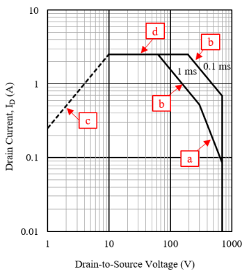
The SOA of a semiconductor device is normally defined by an ambient temperature, TA = 25 ℃, based on the premise that an infinite heatsink is being used. This definition is close to an ideal condition with an adequate cooling capability (e.g., forced air or water cooling). So please pay attention when designing your actual equipment.
In actual equipment design, please be sure to derate an actual operating temperature obtained from the semiconductor device, according to the temperature derating curve of allowable power dissipation with the allowable current of the SOA specified in the corresponding semiconductor device specification set as 100%.
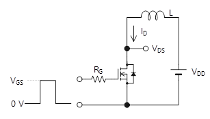
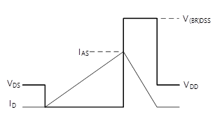
3) Avalanche Energy Capability
Semiconductor devices may break down instantly after a maximum rated voltage is exceeded. However, we guarantee that our power MOSFETs can withstand up to a certain amount of energy above their maximum rated voltage. The amount of energy in which a device can withstand is called avalanche energy.
Avalanche energy capability is a generic term for the withstand capabilities of single-pulse avalanche energy (EAS) and repetitive-pulse avalanche energy (EAR). The EAS capability we guarantee is defined by a time product of the avalanche current (IAS) that can be passed only once, and is expressed by the equation below:
Measurement of Avalanche Energy
(a) Measurement Circuit
(b) Switching Waveform
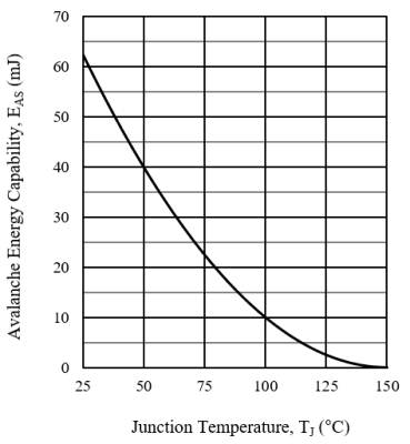
In actual equipment design, as is the case in the SOA, please be sure to derate an actual operating temperature obtained from the semiconductor device, according to the temperature derating curve of the avalanche energy capability (EAS) with the maximum rated EAS value set as 100%. Please also note that the x-axis in a temperature derating curve of avalanche energy capability normally represents a junction temperature of the semiconductor device.
Example Curve: Avalanche Energy vs. Junction Temperature
4) Secondary Breakdown Phenomenon in Transistor
As shown in the figure below, when a voltage keeps increasing even after primary breakdown, it suddenly shifts to a low-impedance region and a current drastically increases. This phenomenon is called secondary breakdown. The secondary breakdown is occasionally abbreviated as S/B.
Characteristics of Secondary Breakdown in Bipolar Transistor
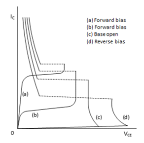
The secondary breakdown is previously regarded as a phenomenon specific to bipolar transistors and is not considered in designing unipolar transistors such as a power MOSFET. Recently, however, it has become commonly accepted to consider the secondary breakdown in power MOSFETs. The smaller the power MOSFET has become to reduce on-resistance, the lower the secondary breakdown point has dropped to the level at which an SOA curve is closer.
A secondary breakdown phenomenon occurs when a current and an electric field concentrate on part of a semiconductor device (element) and generates heat by a locally increased current density. Such local heating produces a hot spot, thus inducing a decrease in the impedance of the hot spot and a further increase in the current. This sequence of reactions , called thermal runaway, will lead to deterioration or breakdown of the semiconductor device.
Shifting into the low-impedance region only takes several microseconds or less, so the semiconductor device will break immediately after the secondary breakdown occurs.
5.3 Life and Failure Rate
1) Design Life of Device
A bathtub curve is a graphical representation to depict changes in the failure rate of equipment or an electronic component.
Normally, a life of a semiconductor device inversely relates to an operating temperature, which means that certain temperature settings will shortens a random failure period and accelerates the life to enter a wear-out failure period earlier. If the semiconductor device in use enters its wear-out failure period (i.e., end-of-life phase) within an expected equipment life period, the equipment may suddenly start to have failures more often when a certain period elapses once marketed.
But you can avoid such situation by applying proper derating to the semiconductor device (especially for temperature) and by designing your equipment so that the semiconductor device will not enter its wear-out failure period within the expected equipment life.
.
Bathtub Curve
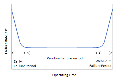
Especially when it comes to power semiconductor devices, an element itself has a large amount of heat generation and its life period greatly varies with a junction temperature during use. Accordingly, it is important to perform temperature derating with not only overvoltage surge and external noise but also life taken into account. For more details about derating and life, please see Section 3.4, “Acceleration Models and Derating” in the Quality and Reliability Information. For semiconductor devices like LEDs and ICs, please pay sufficient attention to the changes in electrical characteristics due to operating or environmental conditions so that your device will not cause abnormal operations.
The design life of general consumer equipment enormously differs depending on its application or sales price. Smartphones and personal computers can be replaced based on equipment functions or changes in equipment performance, not on equipment life periods. Some equipment, whose functional life ends prior to its physical life, is designed such that cost comes first and a life shortens. Some industrial equipment, on the other hand, is designed such that cost comes last but a life lengthens. It is your sole responsibility to take life-extending measures such as temperature derating according to the design life of your equipment. The equipment or devices that are integrated with buildings (e.g., household or building equipment) mostly require a long functional life and are thus designed to have a target decades-long design life. When you consider using our semiconductor devices in long-life applications similar to the ones above, please be sure to contact us in advance and then give adequate consideration to life-extending designs. In particular, when your application requires an extended period of use or an operation at high temperature, please pay sufficient attention.
Most of our semiconductor devices, except for special ones, are designed to have a target life of approximately 10 years when used intermittently for 8 hours a day.
2) Target Failure Rate of Equipment
We carry out strict and close inspection to remove initial failure or defective products. As defects and failures are inherent in our semiconductor devices at a certain rate, however, it is difficult to completely eliminate the occurrence of failures that surface through actual use. When you consider using our semiconductor devices for general consumer use in the equipment premised on zero-defect manufacturing, it is your sole responsibility to take measures (e.g., aging test, burn-in test) for removing early failures represented by a bathtub curve.
5.4 Thermal Design
When a semiconductor device is being used, it is highly important how the heat generated inside the semiconductor device is radiated effectively in order to keep a junction temperature during operation below its maximum rating. This requires appropriate thermal management, i.e., understanding the structure of the semiconductor device and selecting a proper heatsink. For proper heatsink design, please make sure that conditions such as heat dissipation and operating temperature are sufficiently considered. Not only using the semiconductor device within its maximum rated junction temperature (as junction temperature and life are closely and mutually correlated), but also applying temperature derating to ensure the device’s design life is one of the key points in designing. Because using the semiconductor device under the condition with adequate margins directly leads to reliability design.
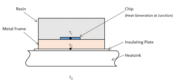
We will describe a semiconductor device supplied in the package with a heatsink as an example here .
1) Allowable Power Dissipation and Thermal Equivalent Circuit
The allowable power dissipation, PD(MAX), of the semiconductor device is specified so that the junction temperature during operation does not exceed the maximum junction temperature, TJ(MAX). And PD depends on the thermal resistance from the junction to the ambient (junction-to-ambient), θJA.
When the thermal stability of a bias circuit is ideal, the allowable power dissipation can be defined by the following equation:
The heat generated at the junction is transferred through a metal frame to the heatsink and is then radiated to the ambient by a cooling medium (e.g., by air when air cooling is employed). Below is the sectional diagram of the semiconductor device.
Below is the thermal equivalent circuit representing an electric circuit when a heat flow is considered same as a current flow.
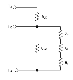
Where:
TJ = Junction temperature
TA= Ambient temperature
TC = Case Temperature
θJC = Junction-to-case thermal resistance
θCA = Case-to-ambient thermal resistance
θc = Contact thermal resistance of case
θi = Thermal resistance of insulating plate
θf Thermal resistance of heatsink
The thermal resistance from the junction to the outside air is defined by the following equation:
In each thermal resistance, θCA is determined by the shape or material of the semiconductor device, which becomes extremely larger than θc, θi, and θf. Hence, the simplified equation is used from a practical standpoint. These thermal resistance values are the constants determined by individual heat dissipation conditions and semiconductor devices.
2) Thermal Resistance
This section explains the following parameters: θJC・θc・θi・θf.
- Junction-to-Case Thermal Tesistance: θJC
The thermal resistance from the junction to the outside air (junction-to-case), θJC, is determined by the structure of the semiconductor device. For the semiconductor devices having an identical structure, this junction-to-case thermal resistance is a constant value regardless of cooling conditions. When measuring θJC, please maintain the case at a constant temperature by forced cooling (e.g., water cooling).
The allowable power dissipation of the semiconductor device at a constant temperature can be defined by the following equation:
The point to be measured for determining a thermal resistance value varies among packages. So please refer to the corresponding data sheet etc.
- Contact Thermal Resistance of Case: θc
The contact thermal resistance, θc, is determined by the states of a contacting portion as follows: flatness and roughness of a contacting surface between the semiconductor device’s metal frame and heatsink; contacting area; and tightening torque. The graph below shows a typical example of the relationship between tightening torque and contact thermal resistance.
Reference: Tightening Torque vs. Thermal Contact Resistance
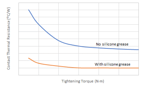
To minimize the contact thermal resistance, be sure to ensure the tightening torque at or above a certain value. Please not that, however, an extremely high torque may cause mechanical stress to the semiconductor device and thus lead to destruction. Therefore, it is strictly required not to exceed the upper limit of a recommended tightening torque specified for each semiconductor device. When the semiconductor device is mounted on a heatsink, applying silicone grease can reduce the torque influence by compensating the roughness and flatness of the contacting surface. This exerts the intended effect with or without an insulating plate.
- Thermal Resistance of Insulating Plate: θi
Some semiconductor devices employ a non-insulating package with internal metal frames are exposed. Depending on the type of these semiconductor devices, the high-voltage part of a chip is mounted on the metal frame. When mounting this type of semiconductor device on a heatsink, please be sure to insert an insulating plate (or insulating sheet) in order to electrically insulate, as a high voltage is applied to the exposed part. In case you omit or fail to implement any insulating measure, a high voltage may be applied to the heatsink and thus cause safety flaws. Or, in case you connect the heatsink to the ground as a noise reduction measure, the chip’s high voltage part may be shorted to the ground and thus destroy the semiconductor device. The thermal resistance of insulating plate, θi, is determined by the property of an insulating plate as follows: material, thickness, area, thermal conductance, and whether silicone grease is used or not.
- Thermal Resistance of Heatsink: θf
The thermal resistance of heatsink, θf, is thermal resistance having characteristics similar to a distribution constant, in the path where heat escapes from the heatsink surface to the surrounding outside air. For the thermal resistance of the heatsink you consider using, please refer to the corresponding catalog etc.
Mounting multiple semiconductor devices on a heatsink will worsen its heat dissipation. Please be sure to reduce electric power per semiconductor device for such configuration.
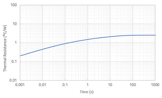
3) Transient Thermal Resistance
When electric power is applied to the semiconductor device, the heat generated in the junction will be transferred or radiated with being varying over time. The transient thermal resistance, θ(t), is thermal resistance showing a transient change until a heat dissipation state becomes stable.
θ(t) can be defined by the equation below, where T0 is the junction temperature before heat generation, TJ(t)is the junction temperature over the time (t), and PC is the power dissipation in the semiconductor device:
The graph below is a typical characteristic curve showing the transient thermal resistance of a semiconductor device.
The transient thermal resistance, θ(t), reaches a value of saturated steady-state thermal resistance when the time (t) elapses long enough.
The saturated steady-state thermal resistance is determined by the heatsink used. However, it becomes the same value regardless of heatsink when a power application time is too short to transfer the heat generated in the junction to the case or heatsink.
Example Curve: Transient Thermal Resistance Characteristic
4) Selection of Heatsink
Please select a heatsink with high flatness of the mounting surface of the semiconductor device and with no scratches. When you consider purchasing a heatsink having screw holes, please select a flat heatsink whose screw holes have no burrs.
When you consider dissipating heat by natural convection, please design so that the fin side of a heatsink is mounted upward from the bottom of your equipment. When you consider forced cooling such as by an air-cooling fan, please be sure to design so that the semiconductor device will remain below its maximum rated temperature even if the fan used fails and stops, or to provide a thermal shutdown circuit.
5) Mounting on Heatsink
Unless otherwise specified, our recommendation is to mount the semiconductor device on a heatsink by screwing.
When you consider mounting with a clip (leaf spring), it is your sole responsibility to decide which clip to use with a sufficient check on variations in the adhesion to the heatsink used.
Please also note that clips are prone to loosen over time and thus require considerations such as a periodic looseness inspection.
5.5. Protection Circuits
1) Selection of Protective Fuse
For power supply circuits, fuses are used for protecting various parts including semiconductor devices. A time-delay (slow-blow) fuse is often used for protecting input circuits. But please be sure to use a fast-blow fuse for protecting our semiconductor devices. In many cases, semiconductor devices break down instantly during the time lag occurred by a fuse. This may result in package cracking or fracturing. In case of such package cracking or fracturing, unusual odors or smokes may be caused. When choosing your protective fuse, please make sure that your design will fully satisfy protection coordination.
2) Thermal Detection and Thermal Shutdown
For semiconductor devices such as ICs, a thermal detection function or thermal shutdown function is incorporated as an overheat protection measure. The “thermal detection” is the function to output a signal from a certain terminal when an IC is overheated. The “thermal shutdown” is the function to stop IC operations when an IC is overheated. As ICs are temperature-sensitive semiconductor devices and known for the difficulty in highly accurate overheat detection. Factors inhibiting accurate overheat detections include the temperature difference between an internal heat-generating part and a detected part, and the time lag from overheat detection to protection activation due to an internal propagation delay. Please note that these functions are intended to increase safety during abnormal operations. For a normal or repeated operation, please do not design your equipment where the thermal detection and thermal shutdown functions are proactively implemented or enabled.
5.6 Confirmation of Noise and Malfunction
1) External Surge Voltage and External Noise
Please design your equipment so that the semiconductor device used will remain within its maximum ratings even if your equipment has an external surge voltage or external noise. For measures against external surge voltage and external noise, please consider adding a noise-absorbing element as needed. Due to variations in manufacturing, actual values such as a withstand capability may vary among our semiconductor devices. When you consider or evaluate your device, please be sure to confirm whether the semiconductor device used will operate within its maximum ratings, not to determine according to actual values yielded by a semiconductor device from a single lot.
2) Latch-up
A latch-up may occur due to any of the following conditions caused by the noise or overvoltage that is externally applied when an IC is in steady-state operation:
- When an input/output terminal voltage exceeds the power supply voltage
- When an input/output terminal voltage drops below the ground voltage
- When an energy exceeding the maximum rating is applied to the power supply terminal
- When a CMOS structure that makes up an IC circuit goes into parasitic operation and the parasitic thyristor formed is turned on due to a rapid rise time of the power supply voltage
In many cases, a latch-up occurs primarily when an overvoltage surge is applied during IC operation. In rare cases, however, a latch-up can also be induced when the ground terminal’s varying electric potential becomes negative and thus puts the IC into an overvoltage state.
The main causes of an overvoltage surge include power supply noise, inductive noise, and static electricity. In design phase, besides PCB component arrangement and pattern routing, please conduct thorough checks on noises (e.g., an inductive noise, electromagnetic noise) via the following tests: injection noise test, impulse test, lightning surge test. Moreover, please add a protection element like a noise-absorbing element as needed.
3) Malfunction Due to Transient Changes
When steep dv/dt or di/dt is applied to a semiconductor device, malfunction or destruction may occur. Therefore, please consider preventing such malfunction by setting a snubber circuit in an appropriate manner.
4) Distortion in Input Signal Waveform
For some semiconductor devices such as ICs, microcontrollers or the like are used for controlling operations by inputting logic signals. If the waveform of an input signal is distorted, normal operations may fail. Please conduct a thorough check on waveforms in design phase.
5) Inappropriate Operations by Microcontroller Sequence
When a microcontroller or the like controls multiple circuits in a sequential order (e.g., a power-on sequence), a semiconductor device may malfunction depending on timing. Please perform a thorough check and evaluation to prevent the semiconductor device you use from the malfunction caused by a transient change or an unexpected operation mode.
5.7. Precautions for Printed Circuit Boards (Printed Wiring Boards)
1) Material and Mounting Position
Various substrate materials are used for PCBs, such as glass epoxy substrates , paper phenolic substrates, ceramic substrates, and more. When choosing your substrate material, please be sure to consider the following parameters: mechanical characteristics, electrical characteristics, heat dissipation property, difference in thermal expansion coefficient between the substrate and mounting components, flame retardance, moisture resistance, workability.
Please note that the PCB warpage induced by soldering or long-term use may apply stress to semiconductor devices or PCB conductive patterns, thus resulting in a disconnection accident. Please also note that the mounting position of a semiconductor device may affect dust to be prone to adhere in some cases, thus leading to an operation failure.
2) Effects from Peripheral Parts
As semiconductor devices are heat-sensitive parts, please design your PCB with attention to the following:
- Heat blown from peripheral parts
- Heat blown from thermal convection by a heatsink
- Heat retained by a moisture-barrier cover
3) Pattern Layouts
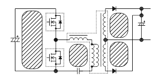
When designing pattern layouts on a PCB, please pay extra attention to trace routing and component arrangements because they will affect malfunction, noise, and loss. It is strictly required to design a pattern having large current to be wide and short as much as possible. Especially for a high-frequency and high-voltage current loop, please be sure to maintain its line impedance as low as possible by designing wider patterns, shorter part-to-part traces, and a smaller internal loop area. The figure below shows an example of high-frequency loops in a primary-side switching power supply circuit (current resonance).
Example: High-frequency Loops
In a power supply circuit, large charging/discharging currents also flow through the line patterns of an input smoothing capacitor. So the same considerations apply to designing power supply circuits. Please place a noise-absorbing element or snubber part near the semiconductor device’s terminal and connect them with a minimal length of traces. Moreover, please provide a sufficient verification so that no inductive noise will occur among adjacent patterns.
4) Hole Sizes and Land Shapes
● For Through-hole Mount Semiconductor Devices
When using a through-hole mount semiconductor device, please design an appropriate margin for the hole sizes on a PCB to be mounted, with careful consideration for the tolerance of terminals. When an automated insertion machine is employed for mounting, please be sure to consider its accuracy of insertion placement. An extremely small size of the holes affects the inserting process of through-hole mount semiconductor devices to be difficult and may thus easily damage conductive patterns on the PCB. Especially when it comes to the semiconductor devices with leadform terminals, please pay extra attention. Please also ensure that the hole pitch (interval) of a PCB and the terminal pitch of a semiconductor device are identical.
● For Surface Mount Semiconductor Devices
When using a surface mount semiconductor device, please design an appropriate land shape on a PCB to be mounted. An ill-designed land shape may prevent solder being insufficiently fed to needed areas and induce a mounting failure or tombstone (Manhattan) phenomenon.
5) Confirmation That Assumes PCB Mounting Process
Semiconductor devices are mounted on PCBs and then incorporated into devices. Please be sure to perform confirmation tests based on your actual mounting and assembly processes. Overvoltage breakdown, i.e., electrical overstress (EOS) is the most common cause of semiconductor device destruction during PCB mounting process or testing process. By conducting thorough checks on the effects to the semiconductor device used, you can determine and take preventive measures to reduce the possible factors of destructive accidents in advance. Such checks include a chattering test at power-on, and a socket insertion/removal test upon connection of the PCB and inspection device.
5.8. After-coating (Secondary Resin Coating and Thermal Curing)
Most of our semiconductor devices, except for some cases, are packaged in exteriors formed with mold resins. However, depending on your equipment use environments, semiconductor devices or PCBs may need further resin coating (after-coating) by your own process in order to fix parts or to improve moisture resistance. Resins used as after-coating include gel materials, rubber materials, mold materials, and others depending on purpose.
It is your sole responsibility whether to implement the after-coating process after fully consulting with a resin manufacturer on the after-coating materials and curing conditions such that excessive stress or thermal stress will not be applied to the semiconductor device used.
5.9. Flame Retardance of Resin and Fire-spreading Prevention
Our semiconductor devices, except for some cases, are packaged in exteriors formed with flame-retardant mold resins (UL94V-0 or equivalent). However, please note that these exteriors are only flame retardant, not non-flammable.
There still be a slight possibility that local heating due to a chip breakdown inside the semiconductor device or melting of internally connected wires associated with the chip breakdown. This may result in smoke or fire generation by the reaction with mold resin components. Therefore, please design your equipment with fire-spreading measures so that the products once marketed will not occur any accidents.
5.10. Safety Design and Fail-safe Design
When designing your device, please be sure to conduct thorough checks such as abnormality testing and worst-case testing so that human injury or death, fire accidents, and social damage can be prevented in case of the destruction of the semiconductor device used.
It is your sole responsibility to decide whether to use the semiconductor device on the basis of sufficient safety design and verification with taking the destruction of the semiconductor device used, component breakdowns, and abnormal operations into account.
Questions or Comments?
Please feel free to contact us if you cannot find the desired product from the lineup.