7 Precautions for Mounting Parts
7.1. Processing of Terminals
1) Bending of Terminals (Lead Forming)
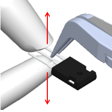
The root portion of terminals of a semiconductor device is an interface between the terminals and mold resin. Therefore, a gap created by the stress applied to this portion will affect product quality due to decreased moisture resistance. When processing terminals, please be careful not to apply stress to the package body by fixing the root of a terminal. When using a tool to fix the root of a terminal, please clamp the root at a slight distance from the package body so that the tool will not contact the package body before and after processing.
Examples of Terminal Processing
Good:
Clamp the root of a terminals at a slight distance from the body, then hold and bend the terminal.
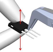
Bad:
Clamp the root of a terminal by the tool at no distance from the body, then hold the body to bend the terminal.
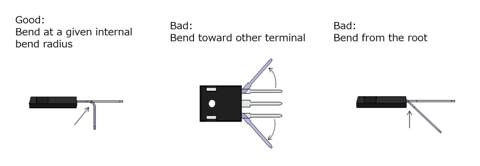
When processing terminals, please do not bend a terminal toward a direction the other terminals are arrayed or from the root, as shown below. Bending a terminal at an acute angle may cause a fracture by vibrations after mounting. Therefore, please define an internal bend radius for the bending portion of terminals. Please note that bending or stretching a terminal repeatedly may also cause a fracture.
Examples of Lead Terminal Processing
2) Stress to Terminals
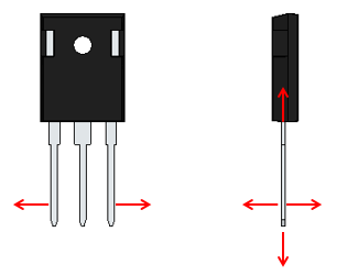
In terminal processing, applying excessive stress to the root of a terminal may break the internal connections of a semiconductor device. Please do not apply stress in any of the directions of the arrows shown below.
Examples of Lead Terminal Processing
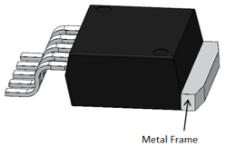
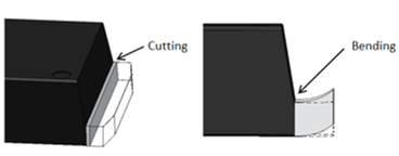
7.2. Cutting or Bending of Metal Frame
For the semiconductor devices supplied in non-insulating packages, please do not cut or bend their exposed metal frames. Otherwise, the semiconductor devices may deteriorate or break down.
Examples of Metal Frame Processing
Non-insulated Semiconductor Device
Bad Processing
7.3. Mounting on Heatsink
1) Handling of Heatsink
Please be sure to handle the mounting surface of a heatsink so that it will not get scratched for ensuring electrical insulation and adequate heat dissipation effects. In particular, power semiconductor devices require a large contacting area for enhanced heat dissipation effects. For this reason, please handle heatsinks carefully to prevent scratches, bows, and twists. Please also prevent the mounting surface from contamination by foreign substances such as a metal piece (metal swarf) produced by cutting or other means.
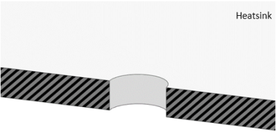
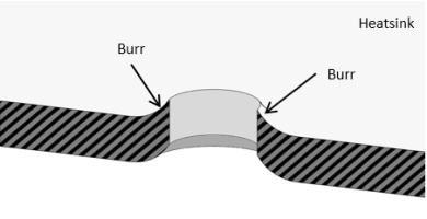
2) Hole Drilling of Heatsink
When drilling a screw hole in a heatsink, please be sure to chamfer a drilled screw hole and make sure that the mounting surface has no burrs produced by pressing or by other means. If the heatsink has a screw hole diameter or chamfer diameter larger than the head diameter of the screw used, stress may be applied to the semiconductor device during tightening. As a result, the semiconductor device’s package and metal frame may deform and lead to deterioration or breakdown. In addition, using tapping screws (not recommended) for screw holes smaller than screw head diameters may cause the following failure factors: actual tightening torque exceeds the recommended value specified for the heatsink; a screw hole in the heatsink is pushed and curled outward by a tap of the screw used. Please note that these failure factors may apply stress to the semiconductor device resulting in a package crack or the like.
Examples of Heatsink Hole Drilling
Good
Bad
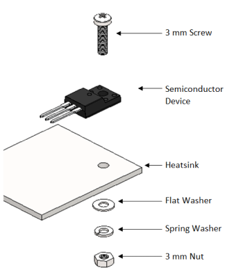
3) Mounting Method
When you mount a semiconductor device on a heatsink, it is recommended to use screws to ensure electrical insulation between the heatsink and adequate heat dissipation effects. For proper mounting, please use a flat washer and spring washer together as illustrated below.
Examples of Semiconductor Device Mounting
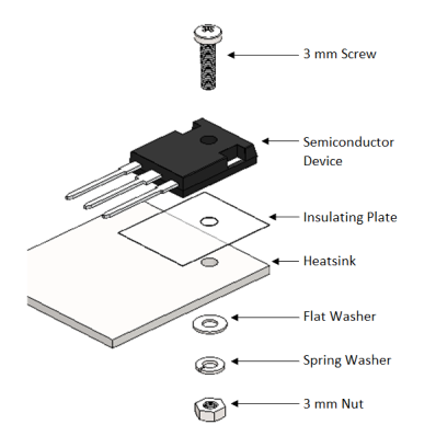
Non-insulated Semiconductor Device
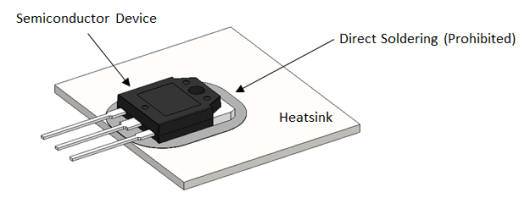
Also, please do not solder the semiconductor device directly to the heatsink.
Bad Example: Soldered Directly to Heatsink
4) Screws for Mounting
● Head Shapes
For screws used for mounting a heatsink, please be sure to select the one with a head shape that provides a flat bearing surface between the contacting surface of a semiconductor device. Please use machine screws having a cross-recessed head or slotted head, i.e., the head shapes equivalent to those of a truss head machine screw and binding head machine screw, specified in JIS-B1111 and JIS-B1101.
Machine Screw Head Shapes Allowed for Use
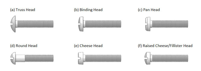
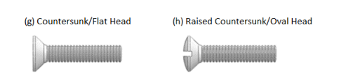
Please do not ever use countersunk head screws because this type of screws may apply abnormal stress to the semiconductor device.
Machine Screw Head Shapes Prohibited for Use
● Point Shapes (Thread Cutting Points )
We do not recommend tapping screws to mount a heatsink (tapping mounting). If you have unavoidable reasons to use tapping screws, please be sure to choose an appropriate type of tapping screws for a screw hole diameter of the heatsink, and to thoroughly check that no abnormal stress will be applied to the semiconductor device during tightening. It is strictly required not to exceed the recommended tightening torque specified for the semiconductor device used.
The tapping screws larger than a mounting hole diameter of the semiconductor device will tap (thread) in the semiconductor device’s package and may thus deteriorate or destroy the semiconductor device. So please do not ever use such screws.
● Material
Before choosing your screw material, please thoroughly consider the tightening method and tightening torque to choose the right one. Please do not ever use brass screws because their heads can be stripped or twisted off due to low mechanical strength. This also may result in loose heatsink mounting and poor heat dissipation effects.
5) Tightening Torque
Before tightening screws to mount a semiconductor device on a heatsink, please be sure to set an appropriate tightening torque. Please be sure to use within the range of the recommended tightening torque. For the recommended tightening torque defined for each product, please refer to the corresponding data sheet. The smaller the tightening torque, the larger the thermal resistance between the semiconductor device and heatsink, hence a decreased heat dissipation effect. An extremely high tightening torque may twist the screw off and deform the insulating plate, resulting in a decreased heat dissipation effect. Moreover, an abnormal strain occurred in the semiconductor device may destroy internal circuit traces or a semiconductor element (chip).
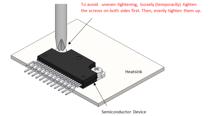
6) Tightening Method
For the semiconductor devices having two screw holes, please be sure to avoid uneven tightening when you mount a heatsink as follows: First, loosely (temporarily) tighten the screws on both sides. Then, evenly tighten the screws up to the recommended tightening torque. Please note that uneven tightening may damage the internal components of the semiconductor device.
Example Tightening: Semiconductor Device with 2 Fixing Points
7) Screwdriver
Our recommendation is to use a manual or electric torque screwdriver for tightening. When using an air screwdriver, please perform a thorough check so that a maximum value of tightening torque variation can fall within the recommended tightening torque.
8) Insulating Plate
When using an insulating plate, please carefully mount it so that contaminants (e.g., foreign substances, dust particles) will not be trapped in contacting surfaces between the semiconductor device and insulating plate, and between the insulating plate and heatsink, respectively. Such contamination may cause the insulating plate used to get scratched, resulting in insulation failures or poor heat dissipation effects. Please note that an insulation failure may also occur if the insulating plate has a pinhole.
9) Silicone Grease
Please apply your silicone grease thinly and uniformly to the contacting surfaces between the semiconductor device and insulating plate, and between the insulating plate and heatsink, respectively. This will reduce the contact thermal resistance of each contacting surface. Please pay extra attention to prevent your silicone grease from contaminated by foreign substances. Contaminated silicone greases may cause the insulating plate used to get scratched, resulting in poor heat dissipation effects or insulation failures.
Depending on the type of silicone greases, the base oil used may intrude into a semiconductor device and thus deteriorate or destroy the semiconductor device’s internal components. Therefore, please be sure to use the heatsink silicone grease that is recommended for resin-encapsulated semiconductors. We recommend the following heatsink silicone greases or equivalent products.
| Product | Manufacturer (As of August 2020) |
|---|---|
| G746 | Shin-Etsu Chemical Co., Ltd. |
| YG6260 | Momentive Performance Materials Inc. |
| SC102 | Dow Toray Co., Ltd. |
7.4. Methods for Mounting on PCB
1) Insertion Method
When inserting a through-hole mount semiconductor device into a PCB, please be sure not to apply excessive stress to the semiconductor device, regardless of whether a heatsink is mounted or not. In particular, please pay extra attention to the semiconductor device’s terminals so that they will not be bent toward a direction the terminals are arrayed or bent from their roots. Please also see Section 7.1, “Processing of Terminals.”
Please also note that squeezing the semiconductor device into or forcefully removing it from the PCB may deteriorate or destroy the semiconductor device.
Some semiconductor devices supplied in DIP packages have slightly opened terminals, which are designed on the assumption of processing by insertion jigs. Therefore, please be sure to use an insertion jig when you insert a DIP-packaged semiconductor device into a PCB.
2) Insertion Position
When inserting a semiconductor device into a PCB, please do not fully insert it up to the roots of its terminals. Please insert the semiconductor device with keeping a proper distance from the PCB.
3) Stress after Insertion
Please note that when heatsink tabs and terminals are inserted into a PCB after the terminals of a semiconductor device are inserted into the PCB, stress may tend to be applied to the semiconductor device’s terminals. Also, please be careful not to apply stress to the semiconductor device during equipment assembly even after the semiconductor device is mounted on the PCB.
4) Mounting of Surface Mount Semiconductor Device (SMD)
When mounting a surface mount semiconductor device (or a surface mount device, abbreviated SMD) on a PCB, please be sure to mount it so that the terminals will be uniformly placed in the center of PCB patterns. Please make sure that the terminals are not misaligned after mounting.
7.5. Soldering
In general, leaving semiconductor devices at a high temperature for a long time may cause deterioration or breakdown. Therefore, please be sure to carry out any processing operations at a low temperature in a short time even during soldering, regardless of which method you employ (e.g., a soldering iron method, a flow soldering method).
Below are the key points you should consider in soldering.
1) Soldering Temperature
Our solder heat resistance tests conform to “JEITA EIAJ ED-4701/300 Stress Test I.” Please be sure to carry out your soldering process under the conditions specified by the above standards. Moreover, resoldering should be done after the semiconductor device once soldered has sufficiently cooled.
When mounting through-hole mount semiconductor devices by flow soldering, please be sure not to dip them into solder liquid.
2) Surface Mount Semiconductor Device (SMD): Soldering Conditions
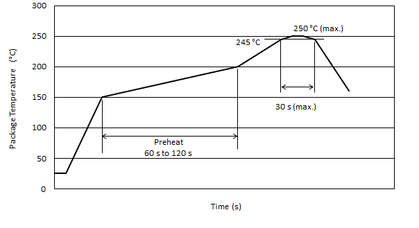
Before mounting a surface mount semiconductor device by flow or reflow soldering, please perform a preheat treatment to mitigate negative effects by abrupt thermal changes. An abrupt temperature rise may cause temperature differences across the semiconductor device’s package, resulting in package bowing or internal component damage. The graph below is a typical reflow profile. Please note that a recommended reflow profile differs among semiconductor device types and package sizes.
Reference: Reflow Profile
3) Surface Mount Semiconductor Device (SMD): Package Cracking
For surface mount semiconductor devices, please keep their expiration dates even if they are moisture-proof packed. When a long-stored or moisture-absorbed semiconductor device is mounted by flow or reflow soldering, its mold resin swells due to the water vapor produced by internal moisture. When the water vapor is further released outwardly from an interfacial delamination part, cracking occurs in the mold resin. Such swelling or cracking of the mold resin correlates to the amount of moisture absorbed. When the semiconductor device seems to have absorbed moisture, please perform a baking treatment before solder mounting.
4) Surface Mount Semiconductor Device (SMD): Post-soldering Visual Inspectioin
After mounting a surface mount semiconductor device by flow or reflow soldering, please make sure that none of the following failure modes has occurred:
- Misalignment of terminals or PCB patterns
- Solder bridges formed among terminals or PCB patterns
- Solder balls adhered to terminals or PCB patterns
- Solder wicking on terminals
- Insufficient solder wetting on terminals
- Flux residues around terminals or PCB patterns
- Package swelling, cracking, or fracturing
5) Flux
Fluxes are commonly used for soldering. However, please note that using strong acid or alkaline fluxes may corrode the terminals of a semiconductor device. Our recommendation is to use rosin-based fluxes. Flux residues on a PCB may cause corroded terminals and poor insulation effects, thus resulting in the sources of electronic circuit troubles. Therefore, we recommend you perform a cleaning process after soldering.
7.6. Cleaning
Below are the key points you should consider in solvent cleaning after a semiconductor device is mounted on a PCB. The solvent cleaning is primarily performed to remove contaminants such as a flux.
1) Solvent (Cleaning Solution)
In general, cleaning fluxes requires purified water and cleaning agents such as alcohol-based solvents. When choosing your solvent, please thoroughly consider and evaluate its flammability, toxicity, and corrosivity in addition to cleaning conditions, so that semiconductor devices will not deteriorate or break down.
2) Cleaning Method
Ultrasonic cleaning causes stress to semiconductor devices. And a degree of the stress differs among cleaning tank sizes, frequencies and outputs of a transducer, solvents, and cleaning times. A mechanical resonance point for the internal components (especially bonding wires) of semiconductor devices is normally near several tens of kilohertz (kHz). So please determine your cleaning conditions based on a thorough evaluation with taking this mechanical resonance point into account. In ultrasonic cleaning, please place the semiconductor devices to be cleaned over the transducers as if the semiconductor devices throw a shadow over the transducers. Please also be careful to prevent the transducers from directly contacting the semiconductor devices or PCBs.
3) Cleaning Time
Soaking semiconductor devices in a solvent for a long time may affect their moisture resistance and cause breakdowns. Therefore, please minimize a cleaning time, regardless of which cleaning method you employ (e.g., immersion cleaning, ultrasonic cleaning). The immersion cleaning is a commonly recommended practice for cleaning semiconductor devices.
4) Peel-off of Marking
Marking types of semiconductor devices are primarily categorized into laser markings or ink markings. Ink markings are very sensitive (less resistant to abrasion) and require attention in solvent cleaning. The higher the solvent has cleaning effects, the more the markings will easily peel off. Therefore, please do not rub the marking surfaces of semiconductor devices until the solvent used has dried.
5) Mounting with Socket
We do not recommend you mount through-hole mount semiconductor devices (e.g., DIP package type) to the mounting sockets already installed on PCBs. If you have unavoidable reasons to employ this mounting method, please do not touch semiconductor devices and sockets with bare hands. Please note that the terminals of a semiconductor device or the socket used that oxidized over time may cause operation failures. Moreover, please be sure to take dust-proof measures because long-term use may also cause the semiconductor device to have operation failures due to the dust accumulated on the socket’s insertion portion.
6) Electrostatic Discharge (ESD) Breakdown
When handling ESD-sensitive semiconductor devices, please be sure to take ESD-proof measures to protect the semiconductor devices from ESD breakdown. In particular, in the process of mounting semiconductor devices to heatsinks, ESD breakdown tends to occur frequently as an operator touches the semiconductor devices. This requires more thorough ESD-proof measures. Please also see Section 9, “Measures for Electrostatic Discharge (ESD).”
In the process described above, please use a conductive parts box when you temporarily store the semiconductor devices in order to enhance your protection against ESD breakdown. Moreover, when using a plastic returnable container for process-to-process transfer, please use a conductive returnable container as part of ESD breakdown protection.
Questions or Comments?
Please feel free to contact us if you cannot find the desired product from the lineup.