
Table of Contents (Bottom of This Page)
Part 1. Compound Semiconductors: What are SiC and GaN?
SiC and GaN: Their Characteristics are Superior
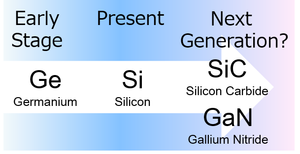
Semiconductors Then and Now ― From Germanium to Silicon
Silicon semiconductor products have evolved over time, with the precision improvement of semiconductor manufacturing equipment and the optimization of device structures and wafer processes. This contributed significantly to downsizing and advancing electronic products in our daily lives.
On the other hand, especially in the power semiconductor field, there have been advances in the element developments and practical applications using compound semiconductors whose physical property values greatly exceed those of silicon-based semiconductors.
SiC and GaN: Compound Power Semiconductors Yield Lower Losses Than Si
From the background mentioned above, the materials such as SiC (silicon carbide) and GaN (gallium nitride) have recently been receiving increased attention.
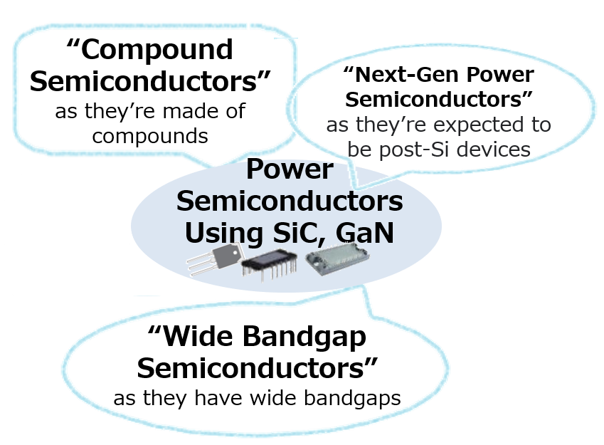
Silicon is a single chemical substance; in contrast, SiC is a compound of carbon with silicon, and GaN is a compound of gallium with nitrogen. For this reason, the semiconductors produced using these compounds are called “Compound Semiconductors.”
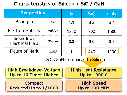
Moreover, SiC and GaN provide bandgaps wider than that of silicon (Si: 1.1 eV, SiC: 3.3 eV, GaN: 3.4 eV), so they are also called “Wide-Bandgap Semiconductors.”
The wide-bandgap semiconductors are characterized by high dielectric breakdown field strength, thus allowing the breakdown voltage same as silicon with a withstand voltage layer much thinner than that of silicon.
With great expectations to be a role to lead future generations, these semiconductors are sometimes called “Next-Generation Power Semiconductors,” too.
SiC and GaN: Their Physical Characteristics are Excellent
Compared to silicon, SiC and GaN—not only as wide-bandgap semiconductors but also as materials themselves—have revealed their outstanding performance levels in the figure of merit (εμeEc3): SiC is 440 times greater, and GaN is 1130 times greater.
To fully utilize these materials, peripheral technologies have been currently under further development. Replacing conventional silicon-based semiconductors with SiC- or GaN-based compound semiconductors will enable more compact and efficient electronic equipment.
In recent years, improvements in the quality of SiC wafer substrates used in semiconductor materials have led to the use of wafers with larger diameters. Accordingly, high-current and low-cost devices have been introduced and are beginning to be adopted in many pieces of equipment.
However, a GaN wafer substrate widely adopts a lateral structure with a GaN active layer formed on a silicon wafer substrate. Although the lateral structure is unsuitable for high voltage and high power applications, this structure allows lower on-resistance and fast switching operations, so it has been used in more and more applications that require compactness. A vertical structure is currently under development, and GaN is expected to achieve high voltage and high power.
Application Ranges Where Si Devices are Possibly Replaced with SiC / GaN Devices
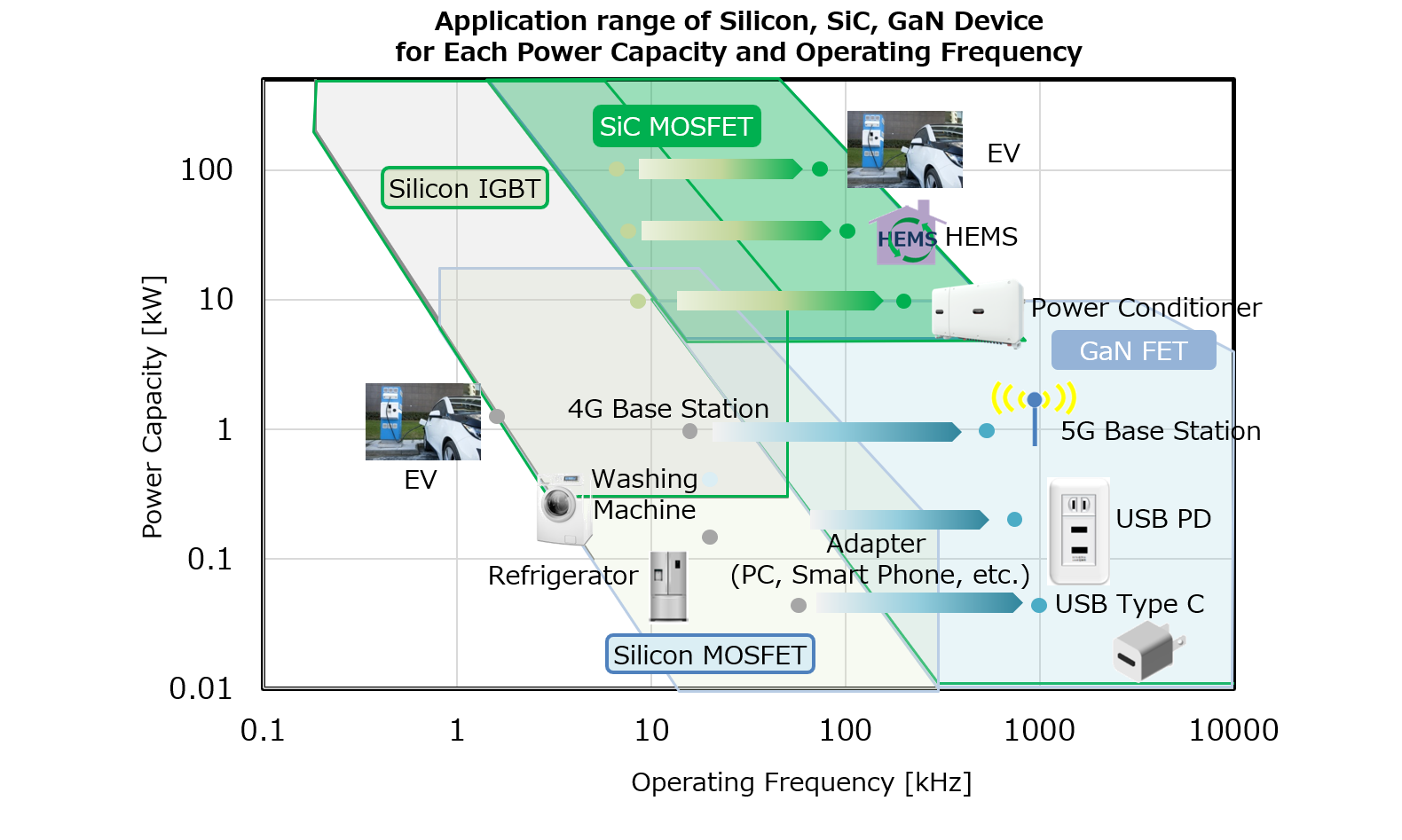
SiC Device has Advantages in Motor Drives and Other High-Voltage / High-Current Applications
SiC is a compound which replaces the half of silicon with carbon. Carbon and silicon are tightly bonded, and its crystal structure is more stable than a single crystal silicon. Therefore, SiC has high dielectric breakdown field strength and thus makes the active layer very thin. This enables a device with a higher breakdown voltage and a lower loss than those of conventional silicon devices.
SiC devices are becoming increasingly popular in the areas of high current and high withstand voltage, as a replacement for silicon IGBTs.
Specifically, they are expanding in the area of 10 kW or more, where there are great advantages in manufacturing smaller and lighter systems, including power conditioners for power generation systems, HEMS for electric homes, and electric vehicles (EV).
GaN Device Has Advantages in Switching Power Supplies and Other Compact / High-Frequency Applications
GaN has an even more stable bond structure and higher dielectric breakdown field strength than SiC.
At present, a GaN device typically consists of a GaN active layer formed on a silicon substrate. GaN devices therefore cannot have breakdown voltages as high as SiC devices do, but they are still suitable for high-frequency applications. When it comes to switching power supplies, by letting them switch at a high frequency, it is possible to downsize inductors and other peripheral components.
GaN devices are expected to be applied in power supplies of 1 kW or less, in fields where compact designs are highly demanded.
For example, GaN devices are more widely used as a power source for base stations of the 5th generation mobile communication systems (5G), which are becoming increasingly popular.
The establishment of the USB Power Delivery (USB-PD) standards also allowed chargers to receive and supply a power up to 100 W through USB cables. As a result, more and more chargers (for smartphones, laptop computers, etc.) have become standardized.
Compact smartphone chargers are long-preferred products, so there has been a demand to provide chargers that will achieve high power and quick charge as well as can support medium-sized electronic equipment like a laptop computer, without changing their current sizes. GaN devices are then here to realize such demand in an optimal manner and are currently accelerating their expansion into many applications.
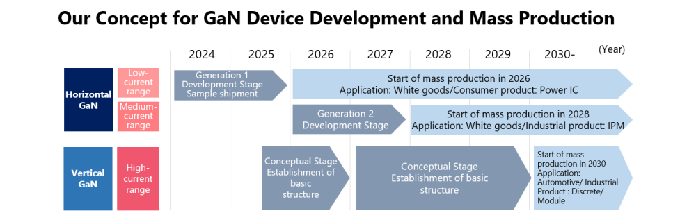
Our Concept for GaN Device
The GaN device market is expected to expand from ¥40.0 billion in 2023 to ¥300.0 billion in 2029. We anticipate that the GaN device market will expand significantly as next-generation power semiconductors focused on the consumer and automotive markets,
and we have started developing lateral GaN devices to cover the low- to medium-current field.
Going forward, we plan to gradually expand the electrical field and applications and to develop and mass produce vertical GaN devices to equip in discrete and module products for automobiles and industrial equipment in the high-current field in 2030.
We will leverage the compound device expertise we have accumulated up to now to promote development and mass production with an emphasis on speed through external collaboration.
Click below to contact us about our products

 Part 2. Applications Where SiC and GaN Devices are Expected to be Used
In the following page, we will introduce nine applications where next-generation power semiconductors are expected to be adopted.

Part 1.
Compound Semiconductors: What Are SiC and GaN?
■ Characteristic Of SiC And GaN Devices
■ Application Of SiC and GaN Devices To Replace Silicon Devices
Part 2.
Application Of SiC And GaN Devices
■ 9 Applications Where SiC And GaN Devices Are Expected To Be Used
Questions or Comments?
Please feel free to contact us if you cannot find the desired product from the lineup.