Factors that Cause IGBT Destruction
Safe Operating Area (SOA) Destruction
The Safe Operating Area (SOA) is divided into a forward bias safe operating area and a reverse bias safe operating area. Exceeding the limited area of the forward bias safe operating area or the reverse bias safe operating area can cause the IGBT to generate abnormal heat, resulting in IGBT destruction.
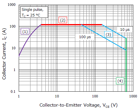
The data sheet provides the safe operating area graph under the ideal conditions (single pulse, TC = 25°C, etc.). Use the IGBT within the safe operating area by derating the graph to the actual operating conditions. For derating, click here.
Forward Bias Safe Operating Area (FBSOA)
The Forward Bias Safe Operating Area (FBSOA) is the range of current and voltage that an IGBT can be used without deterioration or destruction during the IGBT turn-on. The forward bias safe operating area is divided by the following limits.
(1) The area limited by collector-to-emitter saturation voltage, VCE(SAT)(2) The area limited by the maximum rated value of collector current
(3) The area limited by the maximum rated value of junction temperature (thermally limited area)
(4) The area limited by the maximum rated value of collector-to-emitter voltage, VCE
Reverse Bias Safe Operating Area (RBSOA)
The Reverse Bias Safe Operating Area (RBSOA) is the range of current and voltage that an IGBT can be used without deterioration or destruction during the IGBT turn-off. The reverse bias safe operating area is divided by the following limits.
(1) The area limited by collector-to-emitter saturation voltage, VCE(SAT)(2) The area limited by the maximum rated peak value of collector current
(3) The area limited by characteristics specific to an IGBT
(4) The area limited by the maximum rated value of collector-to-emitter voltage, VCE
Destruction by ESD
The gate pin is sensitive to static electricity. If a static electricity or surge voltage generated by the human body or mounting equipment is applied to the gate and a static electricity capacitance of the gate is exceeded, the IGBT may be destroyed.
Measures
- Connect the human body to the ground by a conductive strap or the like.
- Use conductive table mats on workbenches.
- Connect the equipment to the ground or the like.
For more details on the measures for electrostatic discharge (ESD), click here.
Destruction by Parasitic Oscillation
For more details, see Notes on Connecting in Parallel.
Notes on Connecting in Parallel
The following are the key considerations and the guidelines for connecting IGBTs in parallel.
- To reduce the variation of the collector current, IC, in normal operation, use IGBTs with similar values of collector-to-emitter saturation voltage, VCE(SAT).
- PCB layout patterns include parasitic inductance and impedance. To reduce the variation of the current flowing during transients such as turn-on and turn-off, place IGBTs so that there is no variation due to the pattern.
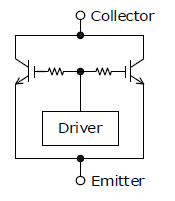
- If the IGBTs connected in parallel are driven by different drivers, the operation of the IGBTs varies due to the effect of the output delay time for each driver. Therefore, drive the IGBTs connected in parallel with one driver as shown in the following figure.
- If IGBTs are connected in parallel without connecting a gate resistor, parasitic oscillation tends to occur. Due to parasitic oscillation, the gate-to-emitter voltage, VGE, exceeds the maximum rated value, or the IGBTs generate heat, which may result in the destruction of the IGBTs. Be sure to connect a gate resistor to each IGBT to suppress parasitic oscillation.
Questions or Comments?
Please feel free to contact us if you cannot find the desired product from the lineup.