IGBT Ratings and Characteristics
Capacitance Characteristics (Cies, Coes, Cres)
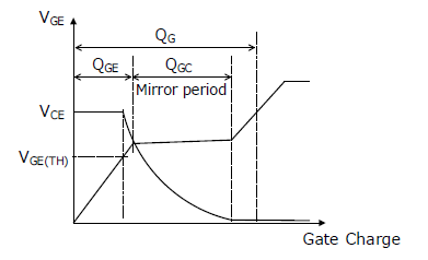
Charge Characteristics (QG, QGE, QGC)
Absolute Maximum Ratings
The absolute maximum ratings are defined as the allowable limits that should not be exceeded, even instantaneously. If one or more of these values are exceeded, the semiconductor device will break. Therefore, it is required to design electronic devices that use semiconductors so that the stress exceeding the values is not applied to semiconductors even instantaneously.
Absolute maximum ratings do not guarantee reliability. Even within the absolute maximum ratings, if the recommended conditions are exceeded, their durability decreases and as a result, semiconductors may not withstand long-term use.
Typical characteristics of the absolute maximum ratings listed in the IGBT data sheet are shown below. The parameters of absolute maximum ratings listed depend on the type of IGBTs.
| Parameter | Symbol | Description |
|---|---|---|
| Collector-to-Emitter Voltage | VCE | Maximum voltage that can be applied between collector and emitter |
| Gate-to-Emitter Voltage | VGE | Maximum voltage that can be applied between gate and emitter |
| Collector Current (DC) | IC | Maximum current that can flow continuously in the collector pin |
| Collector Current (pulse) | IC(PULSE) | Maximum current that can flow in the collector pin for a short time |
| Diode Forward Current (DC) * | IF | Maximum current that can flow continuously in the fast recovery diode |
| Diode Forward Current (pulse) * | IF(PULSE) | Maximum current that can flow through the fast recover diode for a short time |
| Short Circuit Withstand Time | tSC | Maximum time the IGBT can withstand a short circuit |
| Power Dissipation | PD | Allowable maximum power dissipation |
| Operating Junction Temperature | TJ | Allowable maximum temperature in the semiconductor junction in the product |
| Storage Temperature | TSTG | Temperature range at which the product can be stored when the device is not operating |
Electrical Characteristics
Electrical characteristics show the performance of a product by specifying conditions such as temperature, voltage, and current.
The following are typical parameters of electrical characteristics described in the data sheet. The parameters of electrical characteristics to be listed depend on the type of IGBTs.
| Parameter | Symbol | Description | Remarks |
|---|---|---|---|
| Collector-to-Emitter Breakdown Voltage | V(BR)CES | Breakdown voltage between collector and emitter | |
| Collector-to-Emitter Leakage Current | ICES | Collector leakage current when the gate voltage is 0 V | |
| Gate-to-Emitter Leakage Current | IGES | Gate leakage current when the gate voltage is under the specified conditions | |
| Gate Threshold Voltage | VGS(TH) | The gate voltage when the IGBT turns on and the collector current starts to flow | |
| Collector-to-Emitter Saturation Voltage | VCE(SAT) | Collector-emitter voltage when the collector current reaches the specified value with the gate voltage set under the specified conditions. | |
| Input Capacitance | Cies | Sum of gate-to-collector capacitance and gate-to-emitter capacitance | See |
| Output Capacitance | Coes | Sum of gate-to-collector capacitance and collector-to-emitter capacitance | |
| Reverse Transfer Capacitance | Cres | Capacitance between gate and collector | |
| Total Gate Charge | QG | Total charge that the gate voltage increases to the specified voltage from 0 V | See |
| Turn-on Delay Time | td(ON) | Delay time until the IGBT turns on | See |
| Turn-on Rise Time | tr | Rise time until the IGBT turns on | |
| Turn-off Delay Time | td(OFF) | Delay time until the IGBT turns off | |
| Turn-off Fall Time | tf | Fall time until the IGBT turns off | |
| Turn-on Energy | EON | Switching loss at the IGBT turns on | |
| Turn-off Energy | EOFF | Switching loss at the IGBT turns off | |
| Emitter-to-Collector Diode Forward Voltage* |
VF | Voltage drop when forward current flows through the diode | |
| Emitter-to-Collector Diode Reverse Recovery Time* |
trr | Time from when the recovery current flows through the diode to when the recovery current recovers to 90% of the peak value |
Thermal Characteristics
The following are typical parameters of thermal characteristics described in the data sheet. The parameters of thermal characteristics to be listed depend on the type of IGBTs.
| Parameter | Symbol | Description |
|---|---|---|
| IGBT Thermal Resistance | RθJC(IGBT) | Thermal resistance between semiconductor junction and case |
| Diode Thermal Resistance * | RθJC(Di) | Thermal resistance between semiconductor junction and case |
Static Characteristics
This section describes the typical static characteristics of IGBTs.
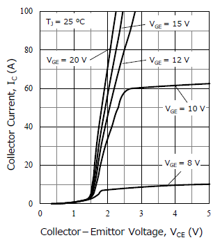
IC-VCE Characteristics
The following figure shows an example of characteristics of the collector current, IC, and the collector-emitter voltage, VCE, at each gate voltage, VGE. IC-VCE characteristics are also called the output characteristics. Due to the structure of IGBTs, a PN junction is generated between the collector and emitter. When the junction potential of the PN junction (VCE = 1.5 V in this characteristic example) is exceeded, the IC starts to flow. The higher the VGE, the lower the VCE when the specified IC is flowing. To reduce conduction loss (IC×VCE), set the IGBT in a region where VCE(SAT) changes are small (generally gate voltage is about 15 V).
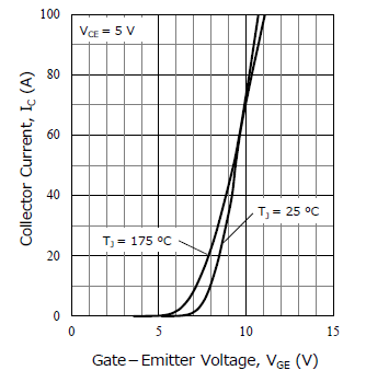
IC-VGE Characteristics
The following figure shows an example of characteristics of the collector current, IC, and the gate-to-emitter voltage, VGE.
In this characteristic example, in the region of VGE < 10 V, the higher the junction temperature, TJ, the lower the VGE when the specified IC is flowing (negative temperature coefficient). Conversely, in the region of VGE ≥ 10 V, the higher the junction temperature, TJ, the higher the VGE when the specified IC is flowing (positive temperature coefficient). To prevent the permanent damage due to heat generation, it is recommended to use the IGBT in the region of positive temperature coefficient.
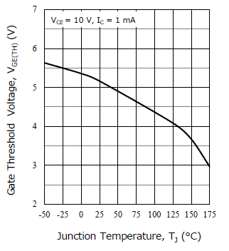
VGE(TH)-TJ Characteristics
The following figure shows an example of characteristics of the gate threshold voltage, VGE(TH), and the junction temperature, TJ.
The higher the TJ, the lower the VGE(TH) (negative temperature coefficient). When the circuit operates and the IGBT temperature becomes high, the IGBT turns on at a low gate voltage. Therefore, changes in VGE(TH) due to temperature characteristics must be taken into account in designing the circuit in order to avoid malfunction due to noise.
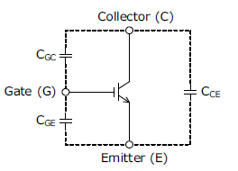
Capacitance Characteristics (Cies, Coes, Cres)
As shown in the following figure, due to the structure of IGBTs, parasitic capacitances (CGC, CGE, CCE) are generated. These parasitic capacitances affect the switching characteristics.
Input Capacitance, Cies
Input capacitance, Cies, affects the delay time. The larger the Cies, the longer the turn-on delay time, td(ON), and the turn-off delay time, td(OFF), because a large amount of charge must be charged/discharged at the IGBT turning on/off. In addition, the larger the Cies, the larger the power loss. Therefore, the IGBT with small Cies is ideal.
Cies is calculated by the following equation.
| Cies = CGE + CGC |
Output Capacitance, Coes
The output capacitance, Coes, affects the turn-off characteristics. When the Coes is large, the voltage change rate, dv/dt, of the collector-to-emitter voltage, VCE, is reduced at the IGBT turn-off, resulting in reducing the influence of noise but increasing the turn-off fall time, tf.
Coes is calculated by the following equation.
| Coes = CCE + CGC |
Reverse Transfer Capacitance, Cres
Reverse transfer capacitance, Cres, is also called mirror capacitance.
Cres affects the high frequency characteristics. The larger the Cres, the more the following characteristics appear.
- The fall time of collector-to-emitter voltage, VCE, at turn-on is long
(The turn-on rise time, tr is long) - The rise time of collector-to-emitter voltage, VCE, at turn-off is long
(The turn-off fall time, tf, is long) - Reverse transfer capacitance, Cres, is calculated by the following equation.
| Cres = CGC |
Charge Characteristics (QG, QGE, QGC)
Total gate charge, QG, gate-to-emitter charge, QGE, and gate-to-collector charge, QGC, are the charges required to drive the IGBT. These affect the switching characteristics. The smaller the value, the smaller the power loss, and the fast switching is achieved.
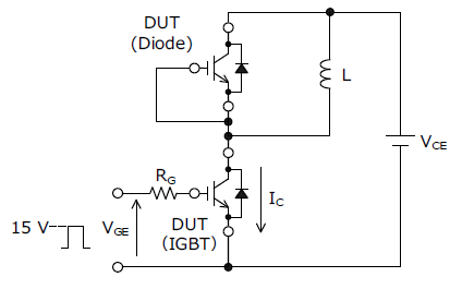
Switching Characteristics (td(ON), tr, td(OFF), tf)
The following figure shows the measurement circuit of switching time.
The following figure shows the switching waveforms.
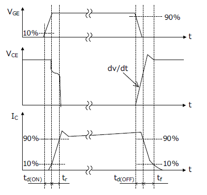
Turn-on Delay Time, td(ON)
Time from 10% of the VGE setting value to 10% of the IC setting value
Turn-on Rise Time,tr
Time from 10% to 90% of the IC setting value
Turn-on Time, tON
The total time of td(ON) and tr
Turn-off Time, td(OFF)
Time from 90% of the VGE setting value to 90% of the IC setting value
Turn-off Fall Time,tf
Time from 90% to 10% of the IC setting value
Turn-off Time, tOFF
The total time of td(OFF) and tf
Short-circuit Characteristics
Short-circuit current, ISC, is the current that flows when an IGBT is shorted. The higher the gate-to-emitter voltage, VGE, the higher the short-circuit current, ISC, thus causing the short circuit withstand time, tSC, to be decreased. The higher the junction temperature, TJ, the lower the tSC.
Fast Recovery Diode
Unlike power MOSFETs, IGBTs do not have body diodes. When using an IGBT to control an inductive load such as a motor, using a product that combines an IGBT and a fast recovery diode (FRD) in one package reduces the number of external components, resulting in reliability improvement of the circuit. Click here for the features of the fast recovery diode.
Questions or Comments?
Please feel free to contact us if you cannot find the desired product from the lineup.