Power MOSFET Ratings and Characteristics
Absolute Maximum Ratings
The absolute maximum ratings are defined as the allowable limits that should not be exceeded, even instantaneously. If one or more of these values are exceeded, the semiconductor device will break. Therefore, it is required to design electronic devices that use semiconductors so that the stress exceeding the values is not applied to semiconductors even instantaneously.
Absolute maximum ratings do not guarantee reliability. Even within the absolute maximum ratings, if the recommended conditions are exceeded, their durability decreases and as a result, semiconductors may not withstand long-term use.
Typical characteristics of the absolute maximum ratings listed in the power MOSFET data sheet are shown below. The parameters of absolute maximum ratings listed depend on the power MOSFET type.
| Parameter | Symbol | Description | Remarks |
|---|---|---|---|
| Drain-to-Source Voltage | VDS | Maximum voltage that can be applied between drain and source | |
| Gate-to-Source Voltage | VGS | Maximum voltage that can be applied between gate and source | Reference |
| Drain Current (DC) | ID | Maximum current that can flow continuously in the drain pin | |
| Drain Current (pulse) | IDM | Maximum current that can flow in the drain pin for a short time | |
| Source-to-Drain Body Diode Forward Current (DC) | IS | Maximum current that can flow continuously in the body diode | |
| Source-to-Drain Body Diode Forward Current (pulse) | ISM | Maximum current that can flow through the body diode for a short time | |
| Avalanche Energy | EAS | Allowable maximum energy at avalanche breakdown by applying a single pulse | Reference |
| Avalanche Current | IAS | Maximum current that can flow at avalanche breakdown | Reference |
| Maximum Drain-to-Source dv/dt | dv/dt1 | Allowable maximum voltage change rate between drain and source | |
| Maximum Diode Recovery dv/dt | dv/dt2 | Allowable maximum voltage change rate at body diode reverse recovery | |
| Maximum Diode Recovery di/dt | di/dt | Allowable maximum current change rate at body diode reverse recovery | |
| Power Dissipation | PD | Allowable maximum power dissipation | |
| Operating Junction Temperature | TJ | Allowable maximum temperature in the semiconductor junction in the product | |
| Storage Temperature | TSTG | Temperature range at which the product can be stored when the device is not operating |
Electrical Characteristics
Electrical characteristics show the performance of a product by specifying conditions such as temperature, voltage, and current.
The following are typical parameters of electrical characteristics described in the data sheet. The parameters of electrical characteristics to be listed depend on the type of power MOSFETs.
| Parameter | Symbol | Description | Remarks |
|---|---|---|---|
| Drain-to-Source Breakdown Voltage | V(BR)DSS | Breakdown voltage between drain and source | Reference |
| Drain-to-Source Leakage Current | IDSS | Drain leakage current when the gate voltage is 0 V | |
| Gate-to-Source Leakage Current | IGSS | Gate leakage current when the gate voltage is under the specified conditions | |
| Gate Threshold Voltage | VGS(TH) | The gate voltage when the power MOSFET turns on and the drain current starts to flow | Reference |
| Drain-to-Source On-resistance | RDS(ON) | Resistance between drain and source when the drain current is flowing | Reference |
| Internal Gate Resistor | RG(INT) | Gate resistor inside the power MOSFET | |
| Input Capacitance | Ciss | Sum of gate-to-drain capacitance and gate-to-source capacitance | Reference |
| Output Capacitance | Coss | Sum of gate-to-drain capacitance and drain-to-source capacitance | |
| Reverse Transfer Capacitance | Crss | Capacitance between gate and drain | |
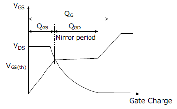
| Total Gate Charge | QG | Total charge that the gate voltage increases to the specified voltage from 0 V | Reference |
| Gate-to-Source Charge | QGS | The charge that the gate voltage reaches mirror voltage from 0 V | |
| Gate-to-Drain Charge | QGD | The charge from when the gate voltage reaches the mirror voltage to when the drain-to-source voltage ≈ 0 V (the charge during the mirror period) | |
| Turn-on Delay Time | td(ON) | Delay time until the power MOSFET turns on | Reference |
| Turn-on Rise Time | tr | Rise time until the power MOSFET turns on | |
| Turn-off Delay Time | td(OFF) | Delay time until the power MOSFET turns off | |
| Turn-off Fall Time | tf | Fall time until the power MOSFET turns on | |
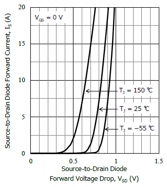
| Source-to-Drain Body Diode Forward Voltage Drop | VSD | Voltage drop when forward current flows through the body diode | Reference |
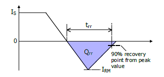
| Source-to-Drain Body Diode Reverse Recovery Time | trr | Time from when the recovery current flows through the body diode to when the recovery current recovers to 90% of the peak value | Reference |
| Source-to-Drain Body Diode Reverse Recovery Charge | Qrr | The charge of flowing current at reverse recovery time | Reference |
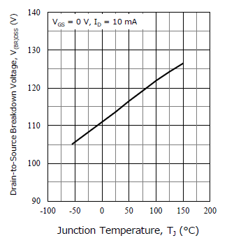
Drain-to-Source Breakdown Voltage, V(BR)DSS
V(BR)DSS is the breakdown voltage between the drain and source. The electrical characteristics are specified in the minimum value, and a margin is applied for the actual value for the safety of circuit operation. However, there is a trade-off relationship between V(BR)DSS and drain-to-source on-resistance, RDS(ON), thus, increasing the margin of V(BR)DSS also increases RDS(ON). Therefore, the margin of V(BR)DSS is generally designed to be as small as possible. V(BR)DSS has a positive temperature coefficient, and the higher the temperature, the higher the V(BR)DSS. The circuit should be designed considering that the V(BR)DSS becomes low at low temperatures.
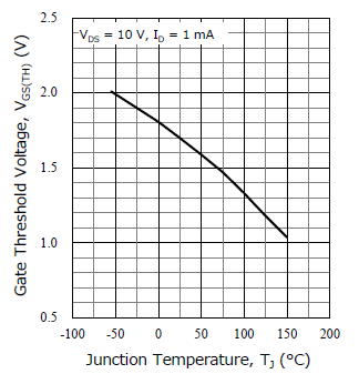
Gate Threshold Voltage, VGS(TH)
VGS(TH) is the voltage between gate and source when the power MOSFET turns on and the drain current, ID, starts to flow. VGS(TH) has a negative temperature coefficient, and the higher the temperature, the lower the VGS(TH). The temperature becomes high during circuit operation and the power MOSFET turns on at a low voltage. Therefore, changes in VGS(TH) due to temperature characteristics must be taken into account in designing the circuit in order to avoid malfunction due to noise.
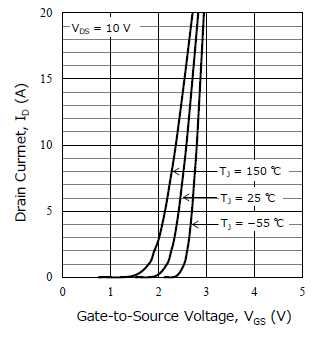
VGS is the applied voltage between gate and source. In order to control the drain current, ID, with VGS, check the ID – VGS characteristics described in the data sheet and set the VGS so that the required ID can flow.
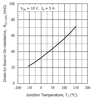
Drain-to-Source On-resistance, RDS(ON)
RDS(ON) is the resistance between the drain and source when the drain current, ID, is flowing. The larger the RDS(ON), the larger the power loss. Therefore, a power MOSFET with small RDS(ON) is ideal. RDS(ON) has a positive temperature coefficient, and the higher the temperature, the higher the RDS(ON). When using at high temperature, consider the change in RDS(ON) due to temperature characteristics. When power MOSFETs are connected in parallel, if there are variations in each RDS(ON), a large amount of current flows through the power MOSFETs with small RDS(ON). However, the flowing current decreases because the RDS(ON) increases due to the temperature rises. The current flowing through each power MOSFET is balanced without the current flowing concentrated on one power MOSFET. This is called the self-stabilizing function of the power MOSFET.
RDS(ON) Resistance
The following figure shows the RDS(ON) resistance of the planar power MOSFET (N-channel).
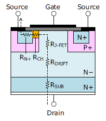
RDS(ON) resistance is calculated by the following equation.
| RDS(ON) = RSUB + RDRIFT + RJ-FET + RCH + RN+ |
Where:
RSUB is substrate resistance,
RDRIFT is drift resistance,
RJ-FET is J-FET resistance,
RCH is channel resistance, and
RN+ is N+ layer resistance.
There is a trade-off relationship between breakdown voltage and RDS(ON), thus, increasing the breakdown voltage also increases RDS(ON). In order to increase the breakdown voltage of the power MOSFET, it is required to thicken the N− layer shown in the above figure. Therefore, the RDS(ON) of a high breakdown voltage power MOSFET depends on the drift resistance, RDRIFT. Conversely, the RDS(ON) of a low breakdown voltage power MOSFET depends more on the channel resistance, RCH, than on RDRIFT.
Capacitance Characteristics (Ciss, Coss, Crss)
As shown in the following figure, due to the structure of power MOSFETs, parasitic capacitances (CGS, CGD, CDS) are generated. These parasitic capacitances affect the switching characteristics.
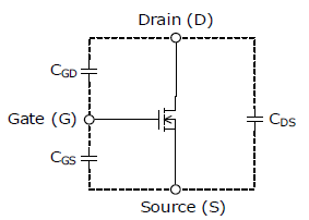
Input Capacitance, Ciss
Input capacitance, Ciss, affects the delay time. When the Ciss is large, the delay time is long because a large amount of charge must be charged/discharged at the power MOSFET turning on/off. The larger the Ciss, the larger the power loss. Therefore, the power MOSFET with small Ciss is ideal.
Ciss is calculated by the following equation.
| Ciss = CGS + CGD |
Output Capacitance, Coss
The output capacitance, Coss, affects the turn-off characteristics. When the Coss is large, the voltage change rate, dv/dt, of the drain-to-source voltage, VDS, is reduced at the power MOSFET turn-off, resulting in reducing the influence of noise but increasing the turn-off fall time, tf.
Coss is calculated by the following equation.
| Coss = CDS + CGD |
Reverse Transfer Capacitance, Crss
Reverse transfer capacitance, Crss is also called mirror capacitance.
Crss affects high frequency characteristics. The larger the Crss, the more the following characteristics appear.
- The fall time of drain-source voltage, VDS, at turn-on is long
(The turn-on rise time, tr is long) - The rise time of drain-source voltage, VDS, at turn-off is long
(The turn-off fall time, tf is long) - Power loss is large
Reverse transfer capacitance, Crss is calculated by the following equation.
| Crss = CGD |
Charge Characteristics (QG, QGS, QGD)
Total Gate Charge, QG, gate-to-source charge, QGS, and gate-to-drain charge, QGD, are the charges required to drive the power MOSFET. These affect the switching characteristics. The smaller the value, the smaller the power loss, and the fast switching is achieved.
Switching Characteristic (td(ON), tr, td(OFF), tf)
The following figure shows the definition of switching time.
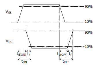
Turn-on Delay Time, td(ON)
Time from 10% of the VGS setting value to 90% of the VDS setting value
Turn-on Rise Time, tr
Time from 90% to 10% of the VDS setting value
Turn-on Time, tON
The total time of td(ON) and tr.
Turn-off Time, td(OFF)
Time from 90% of the VGS setting value to 10% of the VDS setting value
Turn-off Fall Time, tf
Time from 10% to 90% of the VDS setting value
Turn-off Time, tOFF
The total time of td(OFF) and tf.
Body Diode
Due to the structure of power MOSFETs, a body diode is generated between the source and drain. The following figure shows the IS – VSD characteristics of the body diode. The VSD has a negative temperature characteristic and thus the higher the temperature, the lower the VSD.
The following figure shows the reverse recovery characteristics of the body diode. The peak recovery current is defined as IRM. The smaller the reverse recovery time, trr, and the reverse recovery charge, Qrr, the smaller the power loss.
Thermal Characteristic
The following are typical parameters of thermal characteristics described in the data sheet. The parameters of thermal characteristics to be listed depend on the type of power MOSFET.
| Parameter | Symbol | Description |
|---|---|---|
| Thermal Resistance | RθJC | Thermal resistance between semiconductor junction and case |
| RθJA | Thermal resistance between semiconductor junction and ambient |
Questions or Comments?
Please feel free to contact us if you cannot find the desired product from the lineup.