Factors that Cause Power MOSFET Destruction
Destruction by Avalanche Breakdown
Avalanche breakdown occurs when the drain-to-source voltage exceeds the absolute maximum rating to be breakdown voltage, V(BR)DSS, or higher. In the breakdown region, the power MOSFET may be destroyed due to the following factors.
Factors of Destruction
Destruction by Current
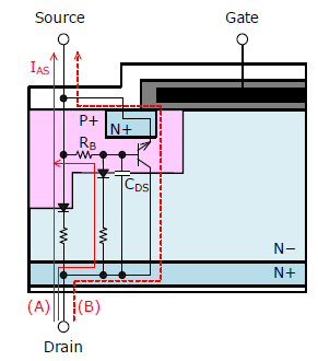
The following figure shows a section view of a planar power MOSFET (N-channel). In the breakdown region, the avalanche current, IAS, flows as shown in (A) in the figure. At this time, a voltage is generated across the base resistor, RB, of the parasitic NPN bipolar transistor. When the voltage exceeds the base-to-emitter voltage that turns on the parasitic NPN bipolar transistor, a current flows as shown in (B) in the figure. At this time, if the drain-to-source voltage is high, the secondary breakdown occurs in the parasitic NPN bipolar transistor, thus, the current flowing through the transistor increases rapidly, resulting in the destruction of power MOSFET.
Destruction by Energy
The power dissipation of energy due to avalanche breakdown causes the temperature to rise. When the junction temperature, TJ, exceeds the absolute maximum rating, the power MOSFET is destroyed.
Decrease in Destruction Capability due to dv/dt
As shown in the following figure, a power MOSFET generates parasitic capacitance, CDS, between drain and source.
As shown in (A) in the figure, the current, I, flows at the power MOSFET turn-off. The current, I, can be calculated by the following equation.
| I = CDS × dv/dt |
Where:
CDS is parasitic capacitance, and
dv/dt is change rate of rise of drain-to-source voltage, VDS
At this time, a voltage (RB×I) is generated across the base resistor ,RB, of the parasitic NPN bipolar transistor. When this voltage exceeds the base-to-emitter voltage that turns on the parasitic NPN bipolar transistor, a current flows as shown in (B) in the figure. As a result, the destruction capability is decreased.
Note that the larger the dv/dt at power MOSFET turn-off, the larger the flowing current, I, and thus, the parasitic NPN bipolar transistor easily turns on.

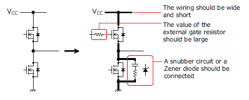
Measures
The following measures are effective in suppressing the destruction caused by the avalanche breakdown.
- The wiring should be as wide and short as possible to reduce the stray inductance.
- The value of the external gate resistor should be large and dv/dt should be small.
- A snubber circuit or a Zener diode should be connected between drain and source to absorb the surge voltage.
Avalanche Energy Measurement
When the drain-to-source voltage exceeds the absolute maximum rating and increases to the breakdown voltage, V(BR)DSS, or higher at the power MOSFET turn-off in the inductive load circuit, avalanche breakdown occurs. The current that flows at this time is called the avalanche current, IAS, and the generated energy is called the avalanche energy, EAS.
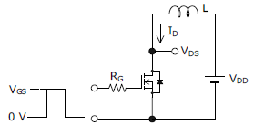
The following figure shows the avalanche energy measurement circuit.
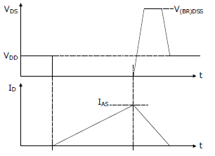
The following figure shows the switching waveforms.
Avalanche energy, EAS, is calculated by the following equation.
| EAS = 1 / 2 × L × IAS2 × V(BR)DSS / V(BR)DSS — VDD |
Where:
EAS is avalanche energy (J),
VDD is power supply voltage (V),
L is inductance (H),
IAS is avalanche current (A), and
V(BR)DSS is drain-to-source breakdown voltage (V).
SOA Destruction
If any of the maximum rating of drain current, the maximum rating of drain-to-source voltage, VDS, and the maximum rating of junction temperature exceeds the safe operating area, the power MOSFET may generate abnormal heat, resulting in power MOSFET destruction.
Safe Operating Area (SOA)
The Safe Operating Area (SOA) is the range of current and voltage that a power MOSFET can be used without deterioration or destruction. The safe operating area is divided by the following limits.
(1) The area limited by the maximum rated value of drain current
(2) The area limited by the maximum value of on-resistance, RDS(ON)
(3) The area limited by the maximum rated value of junction temperature
(4) The area limited by the secondary breakdown
(5) The area limited by the maximum rated value of drain-to-source voltage, VDS
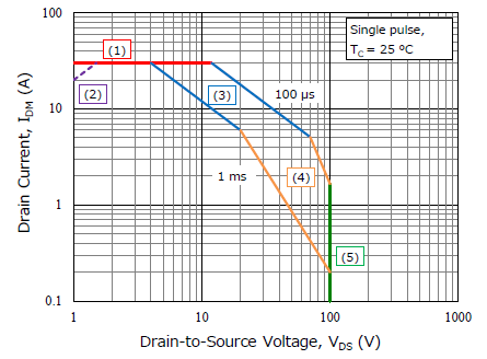
The data sheet describes the safe operating area under the ideal conditions (single pulse, TC = 25 °C, etc.). Use the power MOSFET within the safe operating area by derating the graph to the actual operating conditions. For derating, refer to the link below.
Precautions for Equipment (PCB) Design
Body Diode Destruction
In a circuit that a body diode between source and drain is intentionally used, when the current change rate (di/dt) at the body diode reverses recovery is steep, the voltage change rate (dv/dt2) at this time is also steep. At this time, the parasitic NPN transistor inside the power MOSFET turns on and current flows, which may result in destruction of the power MOSFET.
Measures
- The wiring should be as wide and short as possible to reduce the stray inductance.
- The value of the external gate resistor should be large and dv/dt2 should be small.
- A snubber circuit or a Zener diode should be connected between drain and source to absorb the surge voltage.
Destruction by Parasitic Oscillation
As shown in the following figure, if the power MOSFET is connected in parallel without connecting a gate resistor, parasitic oscillation tends to occur. Due to parasitic oscillation, the gate-to-source voltage, VGS, exceeds the maximum rated value, or the power MOSFET malfunctions and generates heat, which may result in the destruction of the power MOSFET.
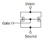
Measures
- The wiring should be as wide and short as possible to reduce the stray inductance.
- A resistor should be connected to the gate of each power MOSFET.
- Ferrite beads should be connected to the gate of each power MOSFET.
Destruction by ESD
The gate pin is sensitive to static electricity. If a static electricity or surge voltage generated by the human body or mounting equipment is applied to the gate and a static electricity capacitance of the gate is exceeded, the power MOSFET may be destroyed.
Measures
- Connect the human body to the ground by a conductive strap or the like.
- Use conductive table mats on workbenches.
- Connect the equipment to the ground.
Questions or Comments?
Please feel free to contact us if you cannot find the desired product from the lineup.